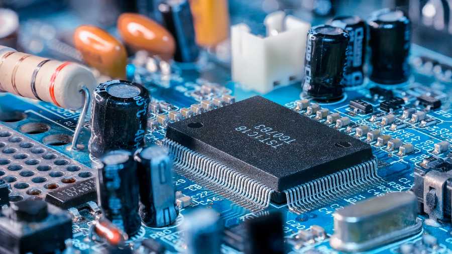
We wake up to messages from our loved ones on our phones. As we commute to work, chips manage the automotive engine. Laptops transform any place into our workplace. Chips are everywhere, silently amplifying our lives manifold.
Moreover, Covid-19 has compressed 10 years of growth in digital demand into a single year due to the lockdown-related conversion of important aspects of life — education, enterprise and entertainment — to digital media. This sudden demand had led to a global chip shortage and sparked a crisis.
The chip shortage has stalled production in the Indian automotive industry while the US, EU and China are shoring up their semiconductor supply chains by pumping in hundreds of billions of US dollars — sparking a technological war dubbed the “chip wars”.
It was in 1874 that German student Ferdinand Braun put a pin on a galena (lead sulfide) crystal and observed that an electric current would pass only in one direction. Thus was “born” a semiconductor rectifier, which could suck out signals from radio waves to power speakers. It brought music to homes from wireless radio stations, spreading joy and cheer!
Semiconductors (silicon, gallium arsenide) are a strange class of materials as they can be turned from insulating to conducting by external controls such as temperature and an electric field. A rectifier acts as an insulator to one direction of current flow driven by an electric field and as a conductor to the opposite direction.
The semiconductor industry is the perfect industry: it turns materials into applications by sheer human ingenuity. Naturally, the rock stars here are engineers and scientists. Why? Well, every two years a memory company doubles its memory product capacity — say, a 32GB flash drive is replaced by a 64GB product — without doubling the cost by “shrinking” each memory transistor in size.
The “shrinking” of transistors is a great innovation. Andy Grove, a Hungarian immigrant to the US, figured out how to oxidise silicon to create the perfect insulator — silicon dioxide. The insulator enabled tiny switches called transistors to be turned on or off without expending much current. This enabled one transistor to operate many other transistors and create a circuit where many transistors could be integrated — or integrated electronics. Shortened, it is Intel — a company that Andy Grove started. Today, chips contain billions of transistors and the cost per transistor has shrunk a million times in the last five decades.
Grove grew a 100-nanometre (nm) layer of silicon dioxide. Today, engineers grow 1nm oxide — that is, three or four atomic layers thick. Such few layers still block currents in billions of transistors, enabling your phone to work flawlessly.
How much is a nanometre? Let’s wait a second — it’s as much as your hair grew in that second. Scientists and engineers built such thin layers in semiconductors with “nature-like” precision.
Closer home, the Indian industry is facing the brunt of a chip shortage. Two things are needed to overcome the challenge. The first is a talented research community. Here, India has emerged as a leader based on astute policy implementation. An aggressive policy to develop a semiconductor research ecosystem gave birth to the Centres of Excellence in Nanoelectronics (CEN), starting with one at IIT Bombay in 2006. By 2011, the CEN research community had become one of the top three contributors to a major international scientific journals, after the US and China. CEN can be considered on a par with similar systems at the University of California, US, or the Chinese Academy of Science in Beijing.
What we now need is to translate innovations into manufacturing solutions. Our MeLoDe labs at IIT Bombay have recently led the translation of the first-ever memory technology in collaboration with the Semi-Conductor Laboratory, Chandigarh. Many such efforts are underway and will succeed.
This brings us to the second element — developing indigenous design and manufacturing infrastructure. Here too, the ministry of electronics has driven the expressions of interest for companies to establish semiconductor manufacturing in India in 2021.
The top labs in India are world-class. Take the IIT Bombay Nano-Fab Facility or its equivalent at other IITs and IISc, Bangalore. They are the perfect place to develop talent. In the US, a researcher toils alone — something that is culturally resonant with the sparse population. There are very few masters students as they are rarely value-for-money where students become productive from their third year onwards.
The ethos at Indian institutions is different. We have a close-knit community of researchers where each PhD student “mentors” many masters students and undergraduates. Thus, top institutes in India are the best place to nurture the next generation of talent and technical leadership.
The global and local demand for India’s future talent — who have learnt the art of innovation — is tremendous. An exciting career awaits those who dare to chase their dreams at the frontiers of deep tech innovation!
The writer is a professor in the department of electrical engineering, IIT Bombay


